Wuxi Electronics Plant
Located in Xishan Economic & Technological Development Zone, Wuxi, we dedicate to the R&D and innovation of Si IGBT and SiC MOS technologies with fully independent intellectual property rights. By integrating upstream and downstream resources, the company has built a complete industrial layout covering chip design and module packaging & testing.
It operates a third-generation semiconductor R&D and manufacturing base in Wuxi and an application center in Baoding. The Wuxi base covers a floor area of approximately 30,000 ㎡, with an annual capacity of 1.2 million automotive-grade power modules.
IGBT Front-end
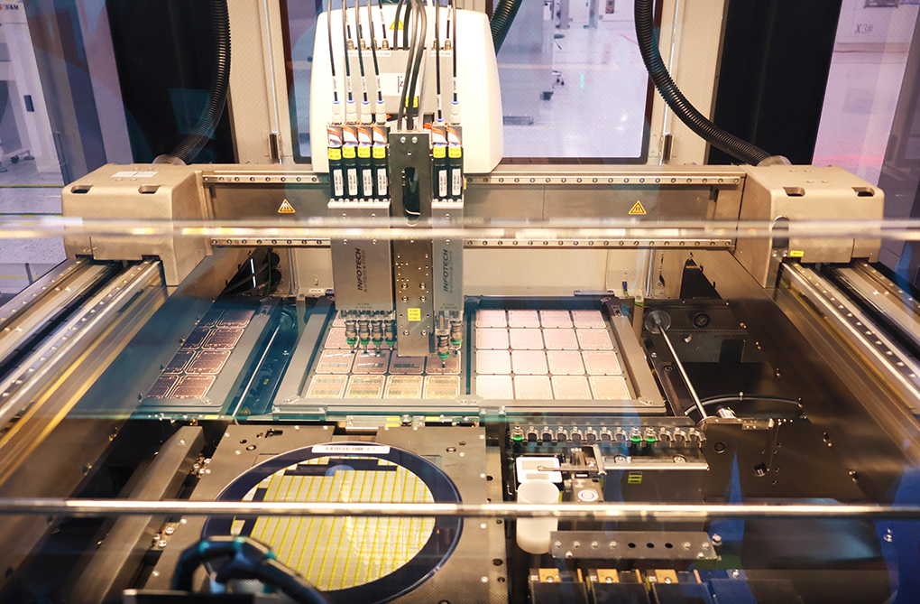
Die Attach
It adopts industry-leading die attach systems with high placement accuracy and precisely controllable bonding pressure, enabling die attachment for IGBT/FRD wafers of various sizes.
The ribbon cutting system achieves high-precision ribbon cutting.
With a high degree of intelligence, it supports accurate chip traceability.
Die Bonding
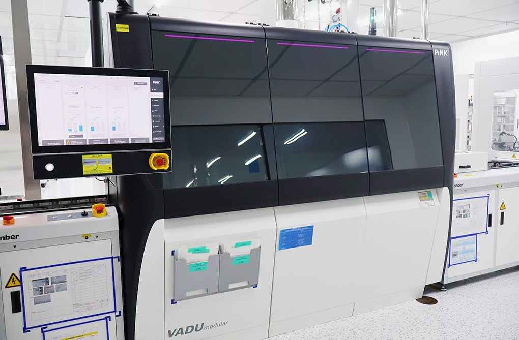
It is supplied by Pink GmbH, Germany, a technology leader in the industry.
This unique three-chamber vacuum soldering furnace features high vacuum level combined with formic acid, which effectively prevents material oxidation and activates bonding interfaces.
It reduces void ratio in die bonding, lowers thermal resistance, and improves reliability and yield.
Its process capabilities are comparable to Infineon, the industry benchmark.

Bonding
This heavy Cu/Al wire bonder is supplied by Germany’s Hesse, a global industry leader, supporting wire diameters from 100 to 600 μm.
Adopting advanced high-power cold ultrasonic bonding, it delivers exceptional process stability.
With 1ms process data sampling, real-time monitoring and charting are realized, clearly reflecting bonding stability and detecting anomalies.
TC bonding
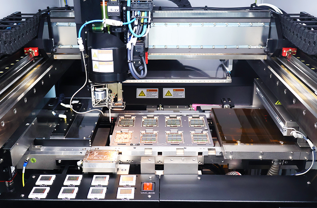
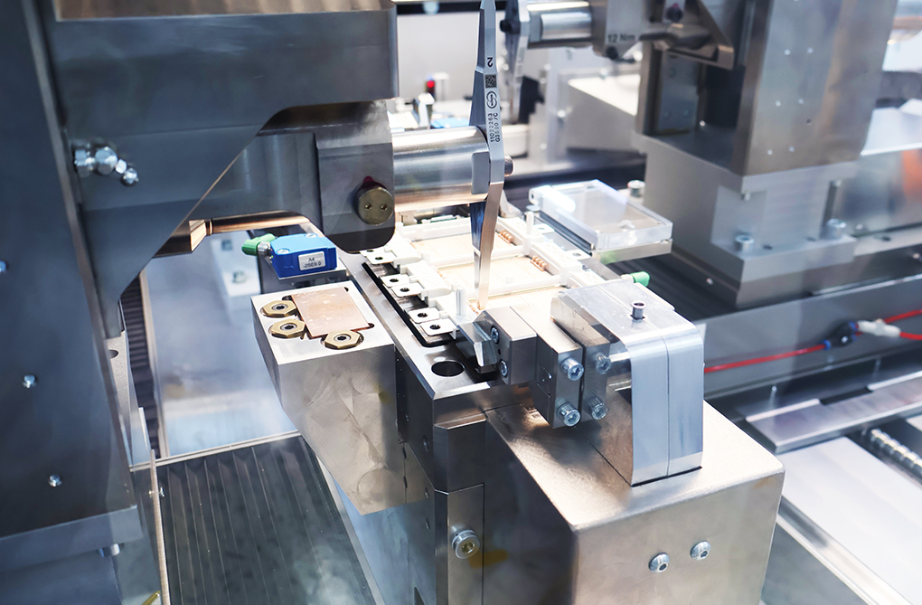
This latest-generation SiC die bonder from Panasonic Semiconductor Equipment (Japan) features an ultrasonic unit in the bonding head.
Ultrasonic energy optimized via DOE is applied to the chip/silver paste interface, achieving rapid micro-bonding. It significantly boosts UPH with a 3-second CT per chip, only 20% of conventional bonders.
Sintering
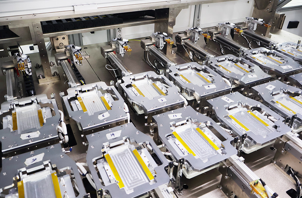
Adopts cutting-edge silver sintering technology with independent pressing heads, ensuring high consistency of sintering strength among different chips on the same substrate.
Post-Potting Process
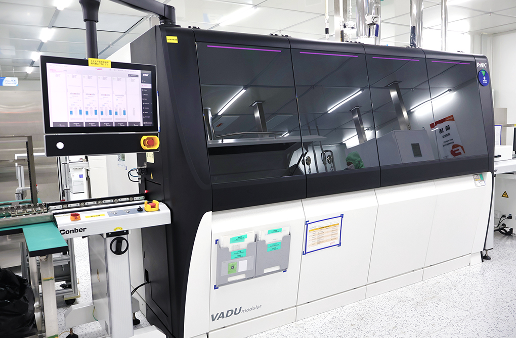
System Soldering Furnace
Provided by Germany’s PINK, a global industry leader, this unique four-chamber vacuum soldering furnace uses high vacuum and formic acid to prevent oxidation, activate interfaces, reduce voids and thermal resistance, and improve reliability and yield.
Its process performance is comparable to Infineon, the industry benchmark.
Terminal Ultrasonic Welding
Supplied by Germany’s Schunk, an industry leader.
It adopts the world’s most advanced standing-wave high-power ultrasonic terminal welding technology, reducing ceramic plate damage caused by welding pressure vs. traditional types, and improving product reliability and yield.
Final Test
Supplied by Italy’s SPEA, a leading test equipment supplier, it is specially designed for high-power module testing with excellent stability.
It supports high/low temperature dynamic, normal temperature static, insulation and on-line RB aging tests for IGBT/SiC half-bridge/full-bridge modules, integrated with laser marking and automatic defective product rejection.
Post-Molding Process
Molding
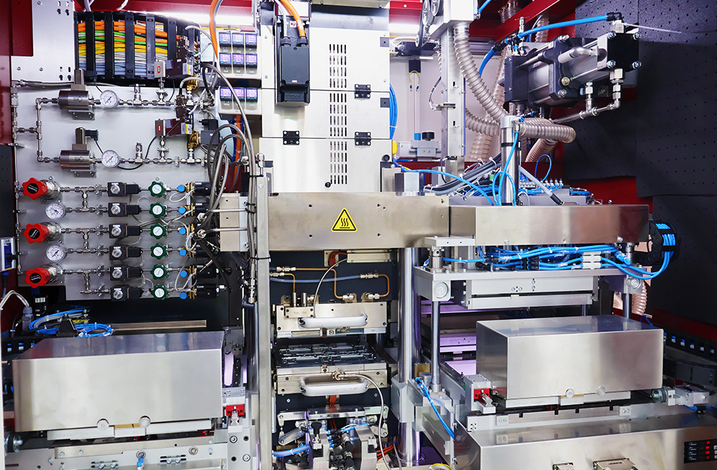
Fully automatic molding equipment encapsulates products with molding compound via transfer molding, delivering reliable physical protection for power modules.
It enables precise control of pressure and temperature, and is compatible with various epoxy molding compounds.
Void and delamination control reaches an industry-leading level.
HTXB
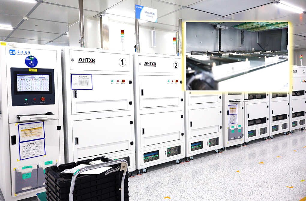
It features an ultra-wide temperature range, is compatible with HTRB and HTGB tests, and can accurately screen out early-stage chip-level failures of power modules.
Adopting the industry’s most advanced hot-plate aging architecture, it improves efficiency by more than 20% compared with traditional oven-type aging equipment.